
DOkA - The first PCB
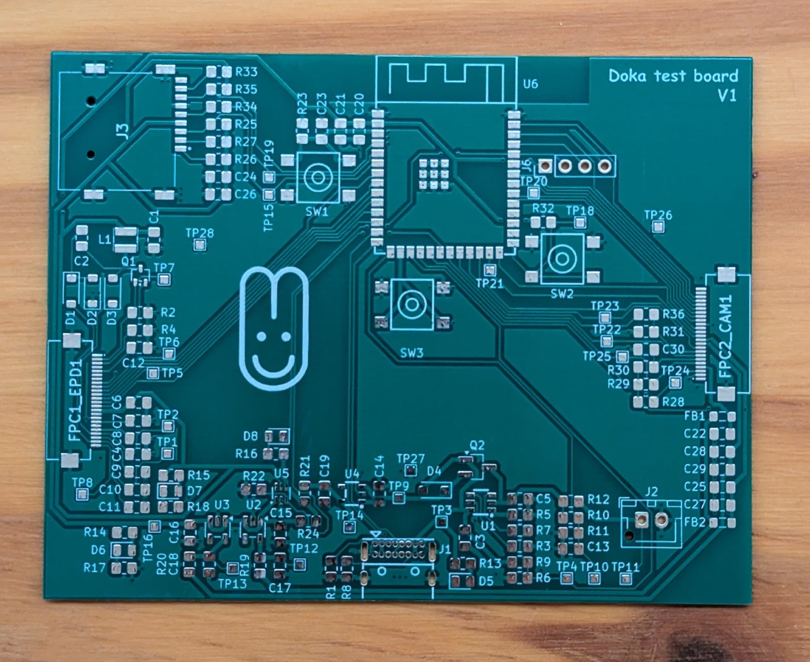
After messing around with the breadboard prototype, it was finally time to dust off my KiCad skills and give DOkA its own PCB. The first PCB is a test version to catch mistakes, the final version comes in a later revision.
The design itself is actually pretty straightforward. It’s just an ESP32-S3 module with some peripherals: a camera module, e-ink screen, SD card and battery charging circuit. As this is a test version, I didn’t confine myself to the final physical dimensions yet, and also included a lot of test points and 0-ohm jumpers to isolate parts of the design. Everything fits comfortably on a 2-layer PCB that I designed in KiCad and had made by JLCPCB.
How the battery complicated everything
Most charge ICs terminate charging when the charge current drops below a certain threshold. But, when a load is “on” during charging, the charger can’t distinguish between the load and charge currents, so it may never terminate charging. That’s why some charging ICs have integrated “power path management”, but they were hard to find in a hand-solderable package, and I wanted to assemble everything myself. So, I implemented this separately using a P-channel MOSFET.
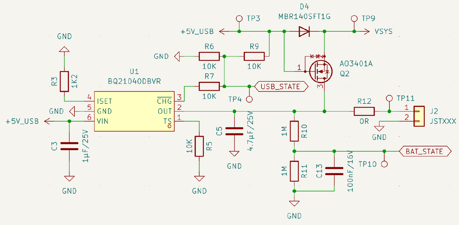
When USB is not connected, the current flows from the battery connector (J2), through the MOSFET (Q2) to the system. The diode (D4) prevents backflow to the USB connector. With USB plugged in, the current flows through the diode to the system. The MOSFET turns off, so the battery is separated from the system.
31 GPIOs sounds like plenty, until it’s not. To save a GPIO, I used a single voltage divider to distinguish between 3 states. With no USB plugged in, USB_STATE simply reads 0V. When the battery is charging, the CHG-port is connected to ground, and R6 and R7 are connected in parallel. USB_STATE then reads around 1.67V. With USB plugged in and the battery no longer charging, CHG is no longer connected to ground. The voltage divider only consists of R6 and R9 and USB_STATE reads 2.5V.
To avoid leakage current, I powered the camera and SD card from a separate 3.3V rail that can be switched off during deep sleep. Initially, I planned to use a load switch for this. A load switch has a controlled “soft start” to avoid large inrush currents that might reset the ESP. As the load switch was out of stock the moment I ordered the components, I temporarily bypassed it using a 0-ohm resistor for testing, which I later replaced by a discrete MOSFET. The e-ink display has its own deep sleep mode, so it stays on the always-on 3.3V rail.
A lesson on FPC connectors
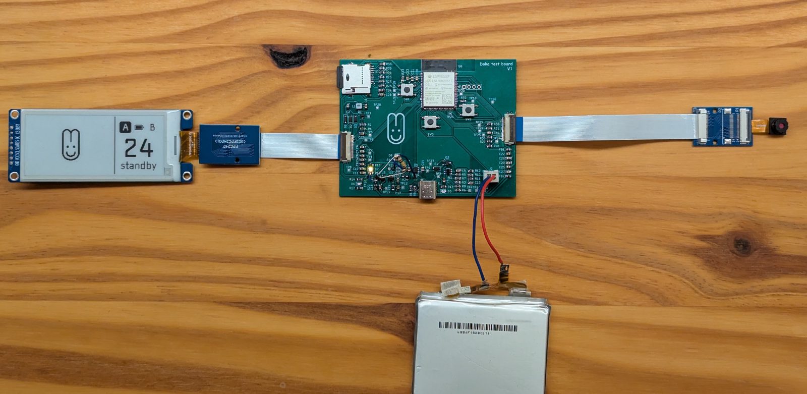
I assembled the PCB section by section. First the power and charging circuit, then the ESP itself, then the e-ink screen, then the SD card and finally the camera, testing each section before moving on.
To my surprise, everything worked as expected. That is, until I assembled the camera. Visually, everything looked fine, but I couldn’t get the camera to work and the 1.5V LDO would become very hot and drop to a voltage of around 0.5V. It didn’t take me long to figure out what went wrong: I had mirrored the pin numbering of the FPC connector. Pin 1 became pin 24 and so on, which shorted the 1.5V LDO to ground. Luckily, this didn’t damage the camera or the LDO.
One way to fix this is to replace the FPC connector with one that has its contacts on the top instead of the bottom. I really didn’t want to go through the headache of soldering an FPC connector again, so I opted for the lazy solution. I ordered an adapter board online that changes the pin order of an FPC connector. Three days later I could continue the testing, and this time everything worked flawlessly.
Finding the leakage current
The last thing I wanted to verify with this PCB was the current draw, especially during deep sleep. To replace the load switch, I soldered a separate MOSFET with pull-up resistor to the board. This looks a bit funky, but it works. When the camera is ready, the board draws around 250mA. This was in line with what I expected. Initially, in deep sleep, the current draw was around 470µA, way higher than the tens of µA range I expected.
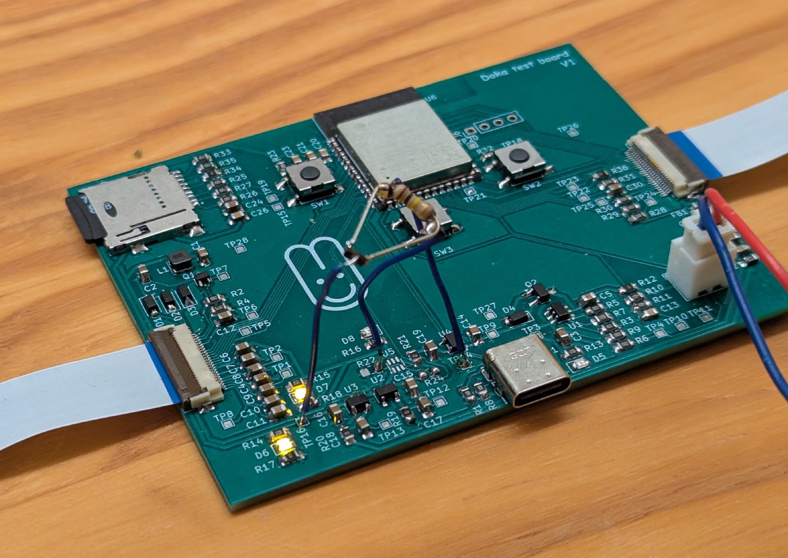
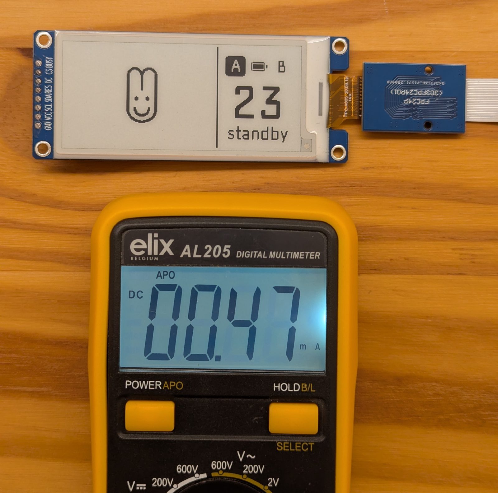
This meant that current was still leaking somewhere. I checked all resistors for any remaining voltage (and thus leakage current), and checked whether the separate 3.3V rail was back-fed somewhere. This was not the case. Eventually, the culprit turned out to be the GPIOs that control the display. These were left floating, causing a leakage current in the display controller. After a short correction in the firmware, the leakage current dropped to around 20µA. Much closer to what I expected.
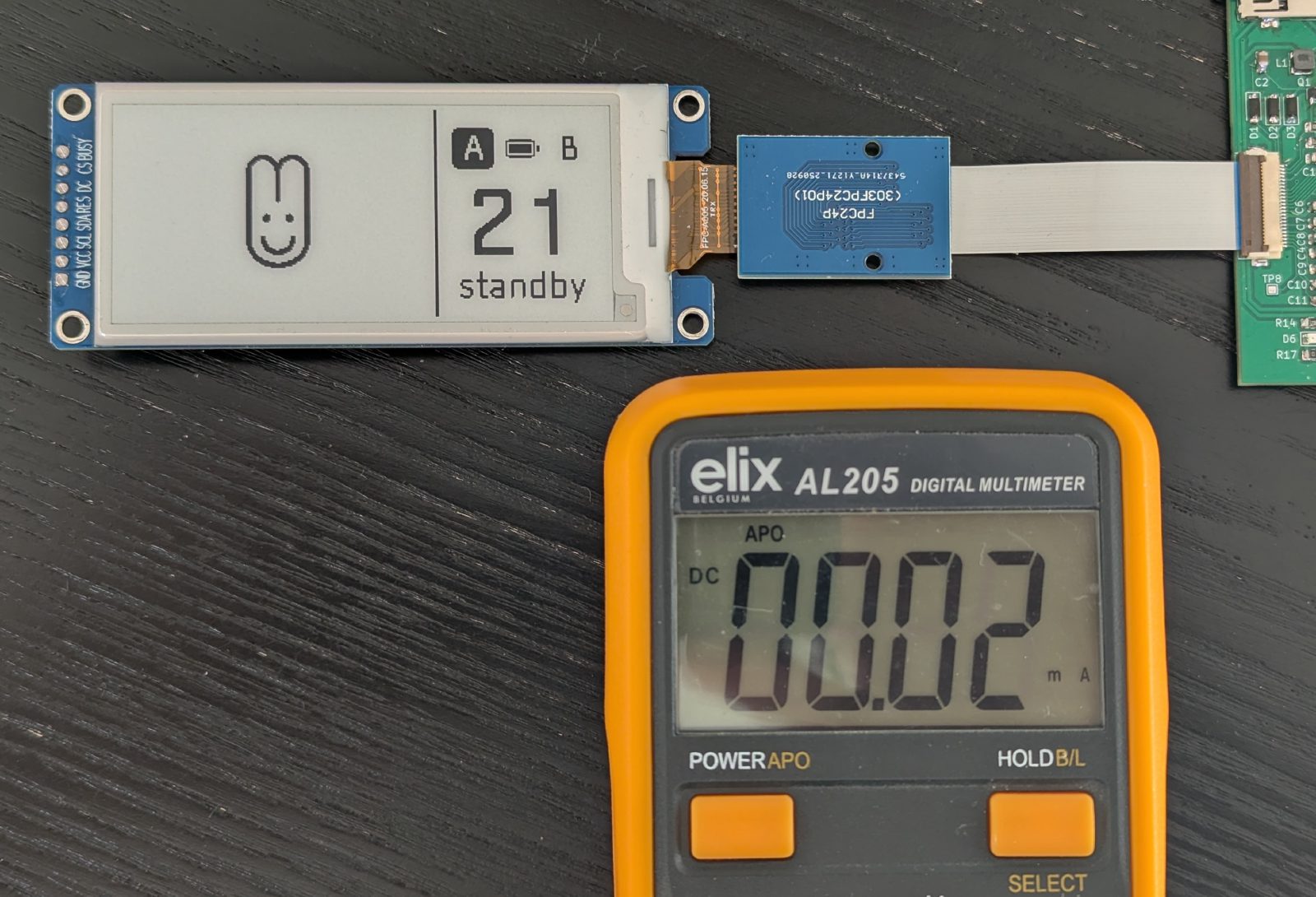
With the 1200mAh battery that I plan to use, this means a theoretical usage time of around 4h, and a standby time of several years. At such low discharge rates however, the self-discharge of the battery becomes more important. The power consumption of the device in the “on” state could be further optimized, e.g. by lowering the CPU frequency and powering off the camera at strategic moments, but for the moment this is still on my to-do list.